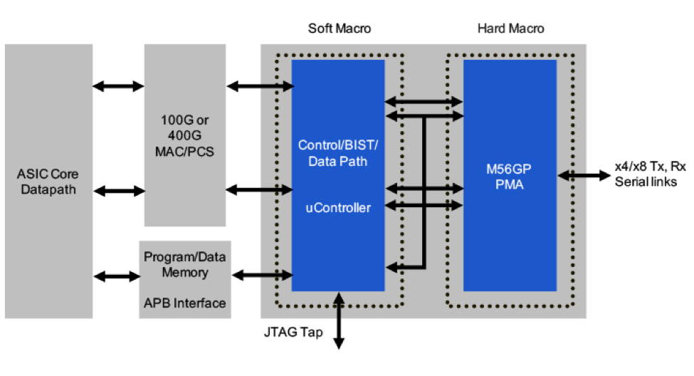
Gary Hilson of the EE Times has written a detailed article about Rambus’ 56G SerDes PHY. As Hilson notes, the analog-to-digital converter (ADC) and (DSP) architecture of Rambus’ 56G SerDes PHY is designed meet the long-reach backplane requirements for the industry transition to 400 GB Ethernet applications. This means it can support scaling to speeds as fast as 112G, which are required in the networking and enterprise segments, such as enterprise server racks that are moving from 100G to 400G.

“Ethernet is moving faster than ever,” Mohit Gupta, senior director of product marketing at Rambus, told the EE Times. “The pace has picked up substantially due to big data, the Internet of Things (IoT) and other trends putting high demands on communication channels. There is already a forum for 112G SerDes speed which will drive the 800G standard.”
According to Gupta, one clear use case is data center deployment by the big four: Facebook, Microsoft, Amazon and Google. In addition, Gupta noted that wireline and wireless communications are guiding Rambus’ memory and interface development. More specifically, the move from 4G to 5G is driving new architectures such as C-RAN, which further pushes SerDes requirements to communicate between remote radio head (RRH) and baseband unit (BBU) from 12G to as high as 48G. As Hilson reports, Rambus will use long-term partner Samsung’s 10nm Low-Power Plus (LLP) process technology for the 56G SerDes PHY, which provides a higher performance and lower power node in comparison to first generation FinFET nodes.
Gupta also told the EE Times that the evolution of memory interfaces for networking applications is being driven by high-bandwidth and low-latency requirements. To be sure, High Bandwidth Memory (HBM) technology that was originally targeted at graphic companies such as NVIDIA and AMD is now being deployed in networking chips and the technology is becoming more accessible as 2.5D integration reaches maturity. Concurrently, on-chip memory continues to be dominated by SRAMs and TCAMs for communication chips.
“SRAM performance still matters a lot for buffers being able to communicate at higher speed as logic is being driven faster,” Gupta explained.
Hilson concluded the article by noting that SerDes PHY IP is one of Rambus’ flagship products, with its Snowbush IP acquisition enabling the company to broaden its offerings.
“Last summer, [Rambus] announced it had developed the first production-ready 3200 Mbps DDR4 PHY available on GLOBALFOUNDRIES’ FX-14 ASIC platform using its power-performance optimized 14nm LPP process. The Rambus DDR4 PHY is part of the company’s comprehensive suite of memory and SerDes interface offerings on 14nm for networking and data center applications,” he added.
Interested in learning more about Rambus’ 56G SerDes PHY? You can check out our product page here and our article archive on the subject here.
