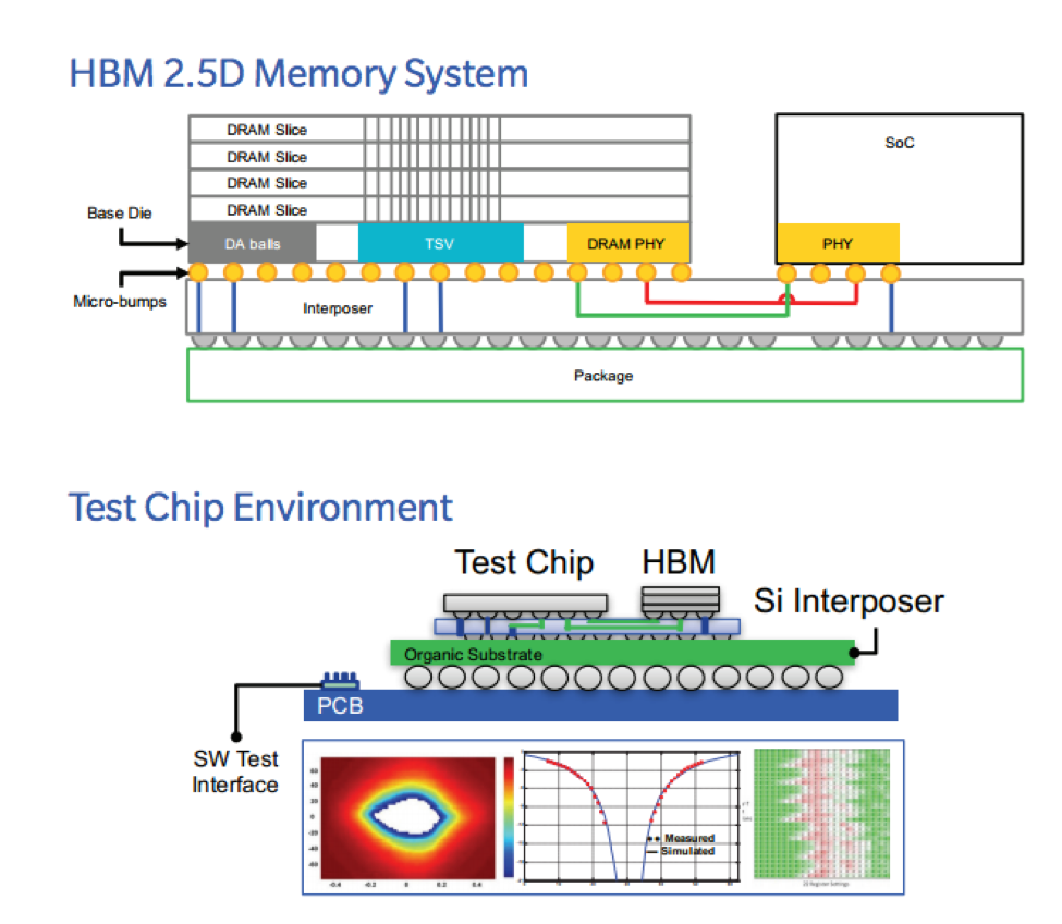
Rambus’ Bill Fuller recently penned an article for Semiconductor Engineering about HBM2 DRAM. As Fuller observes, HBM DRAM is currently used in graphics, high-performance computing (HPC), server, networking and client applications. Recent examples of second-generation HBM deployment include NVIDIA’s Quadro GP100 GPU which is paired with 16GB of stacked (through-silicon via) ECC HBM2 (High Bandwidth Memory) for 720GB/s of bandwidth and Intel’s new Lake Crest CPU which packs 32GB of HBM2.
Read first our primer on:
HBM2E Implementation & Selection – The Ultimate Guide »
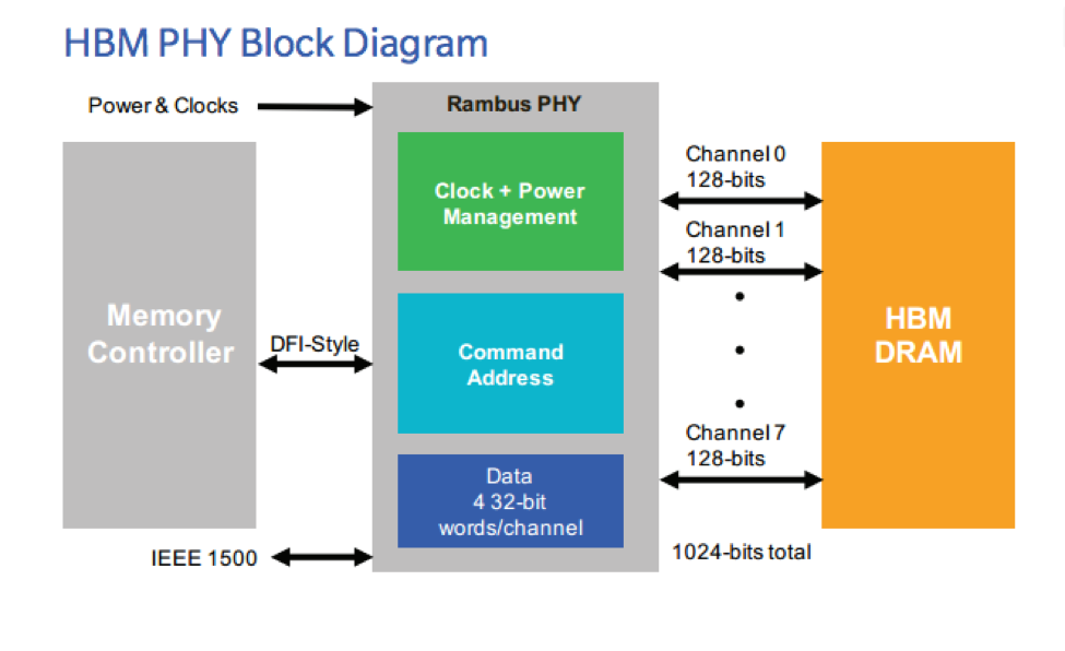
“As system designers look to move higher bandwidth closer to the CPU, HBM2 offers an opportunity to significantly expand memory capacity and maximize local DRAM storage for wider throughput in the data center,” Fuller explained. “Indeed, HBM DRAM architecture increases system memory bandwidth by providing a wide interface to the SoC of 1024 bits. More specifically, second-gen HBM offers a maximum speed of 2Gbits/s, or a total bandwidth of 256Gbytes/s. Although the bit rate is similar to DDR3 at 2.1Gbps, the eight 128-bit channels provide HBM with approximately 15x more bandwidth.”

According to Fuller, HBM2 architecture presents engineers with several unique PHY, chip and subsystem design challenges. For example, although HBM memory is 1,024 bits wide, the interconnect count approaches 1700 when power, ground and other necessary signaling techniques are taken into account. In addition, driving high signal counts affects a wide range of considerations, including power and ground distribution, signal integrity and cross-talk interference.
“Interposer designs – which connect HBM modules to the SoC – are also quite challenging to implement, as signal length needs to be minimized to reduce drive strength requirements and power consumption for the PHY,” Fuller continued. “Similarly, cross-talk should be meticulously analyzed and mitigated, while impedance and ground return paths must be carefully considered to maintain signal integrity and meet timing and eye margin requirements for the HBM PHY interconnect.”
Despite these challenges, says Fuller, an HBM2 system can be effectively designed with robust timing, temperature and voltage margins for high-volume production. However, building a robust, dependable PHY requires careful interposer layout, extensive chip and package simulation and analysis, as well as solid power distribution.
“The interposer can be designed with a reasonable number of signal layers when utilizing small but achievable signal widths. Further analysis shows that side-guard grounding signals are not required. Adequate eye margins can be achieved when careful routing keeps the signal lengths reasonable and multiple signal layer transitions are avoided,” he added.
It should be noted that Rambus recently launched its new High Bandwidth Memory (HBM) Gen2 PHY. Designed for systems that require low latency and high bandwidth memory, the Rambus HBM2 PHY, built on the GLOBALFOUNDRIES advanced 14nm Power Plus (LPP) process technology, is targeted at networking and data center applications.

The PHY is fully compliant with the JEDEC HBM2 standard and supports data rates up to 2000 Mbps per data pin, resulting in a total bandwidth of 256 GB/s. The interface features 8 independent channels, each containing 128 bits for a total data width of 1024 bits, as well as support for a stack height of 2, 4 or 8 DRAMs. The PHY is also designed for a 2.5D system with an interposer for routing signals between the DRAM and PHY.
Key HBM Gen2 PHY product highlights include support for DRAM 2, 4 and 8 stack height, a DFI-style interface to the memory controller, 2.5D interposer connections between the PHY and DRAM, a validated memory controller interface, support for wafer-level and interposer testing, as well as availability with LabStation™ Validation Platform for enhanced bring-up and validation.
Additional features include a flexible delivery of the IP core (works with ASIC/ SoC layout requirements), 8 channels and 16 pseudo-channels, selectable low-power operating states, programmable output impedance, pin programmable support for lane repair, ZQ calibration of output impedance, IEEE 1500 test support, SSO noise reduction, micro-bump pitch matched to the DRAM pitch, east-west orientation (PHY can be placed in corner of die) and a register interface for state observation.
The HBM Gen2 PHY – delivered as a fully characterized hard macro – includes all necessary components for robust operation, such as IO pads, PLL, clock distribution, transmit and receive paths, control logic, power distribution and electrostatic discharge (ESD) protection circuitry.
Interested in learning more about Rambus’ HBM Gen2 PHY? You can check out our product page here and download our product brief here.
