Frank Ferro, Senior Director Product Management at Rambus, and Shane Rau, Senior Research Executive at IDC, recently hosted a webinar that explores the role of tailored DRAM solutions in advancing artificial intelligence. Part three of this four-part series touched on a wide range of topics including the impact of AI on specific hardware systems, training versus inference, and selecting the most appropriate memory for AI/ML. This blog post (part four) takes a closer look at the evolution of HBM and GDDR6, as well as the design tradeoffs and challenges of the two memory types.
The Evolution of HBM
Although HBM2 is currently shipping, standardization and market requirements are pushing HBM to go faster and faster. HBM2 says, Ferro, started off with a two gigabits per second data rate, and has since moved to 3.2, with some companies announcing versions that are even faster.
“We don’t see any end in sight for faster HBM speeds. The next generation of the HBM standard is already being worked on. The industry is pushing very hard to continue to drive the bandwidth up on HBM,” he adds.
Despite its ability to achieve extremely high speeds and bandwidth, Ferro emphasizes that HBM, which utilizes a very wide interface, is still based on DRAM (DDR3-DDR4) technology.
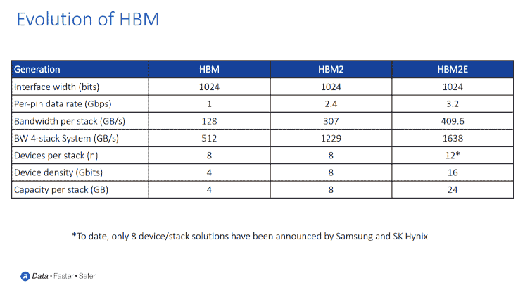
Note: On Sep. 9, 2020, Rambus announced its HBM2E interface could operate at 3.6 Gbps raising bandwidth to 461 GB/s.
“In the slide [above], you can see there’s 1,024 bits that are being used for HBM. Essentially, we are taking really a traditional DRAM and we’re going to go very, very wide on the interface,” he explains.
“You’re going wide and slow if you want to think of it that way, which gives you very good power efficiency and very high bandwidth. These are very good attributes, but you also have to deal with its 2.5D structure.”
Despite its challenges, says Ferro, HBM is the most optimal system for bandwidth and power efficiency. As well, HBM also offers optimal density.
“HBM stacks more traditional DRAMs in a 3D structure. And by stacking, you get both capacity and bandwidth. On this slide [below] in the bottom left hand corner, you can see what an HBM system looks like. You have the HBM DRAM, that’s sitting on top of the silicon interposer connected to the processor,” he elaborates.
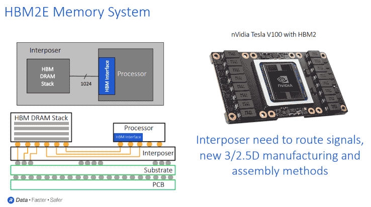
“The HBM DRAM stack, depending on the density you need, could have up to 8 stacks of DRAM. With HBM2E, you can go to a stack of 12 DRAM. Then you connect the DRAM to the CPU through a silicon interposer. Remember you have 1024 data lines that are running through the interposer along with all the control and power and ground lines.”
As well, says Ferro, there are many traces that need to be routed, which is best achieved with a silicon interposer.
“You can see that in a very small footprint you get quite a bit of memory and processing power. On the right-hand side in the slide [above], you see a picture of the processor from NVIDIA that uses four HBMs DRAM stacks. You can also see the four DRAMs are sitting alongside the processor. Again, even with a very small footprint, you get a very large amount of processing power.”
HBM: Design Tradeoffs and Challenges
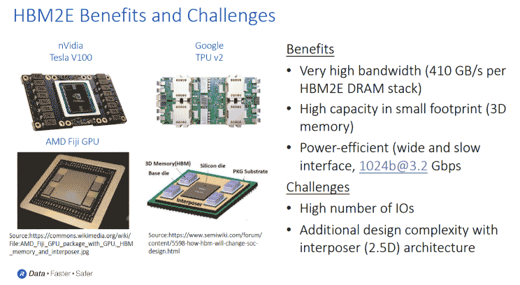
The slide below, says Ferro, illustrates the trade-offs, benefits and challenges of developing an HBM system. On the left side, there are dedicated GPUs and processors like Google’s TPUs that use HBM for their processing power.
“Again, the benefits are very high bandwidth, high capacity and a small footprint. However, you have to build that system. You’ve got to deal with all of these I/Os. You also have to deal with the complexities of the 2.5D structure,” he explains. “Although the industry is maturing from a manufacturing standpoint, HBM is still relatively new because you have to take the silicon die of the DRAM and the silicon die of your processors. You have these two known good dies, and those two known good dies are going to sit on a silicon interposer, which goes into package. It is still relatively new and expensive to develop HBM. Because of the expense, it has given rise to GDDR6.”
The Evolution of GDDR6
According to Ferro, GDDR6 offers a “really good” trade-off between speed, performance, and design complexity versus HBM.
“In the slide [below], you can see it’s a 32-bit interface, again, more traditional interface, very similar to LPDDR, also very similar to DDR as well,” he states.
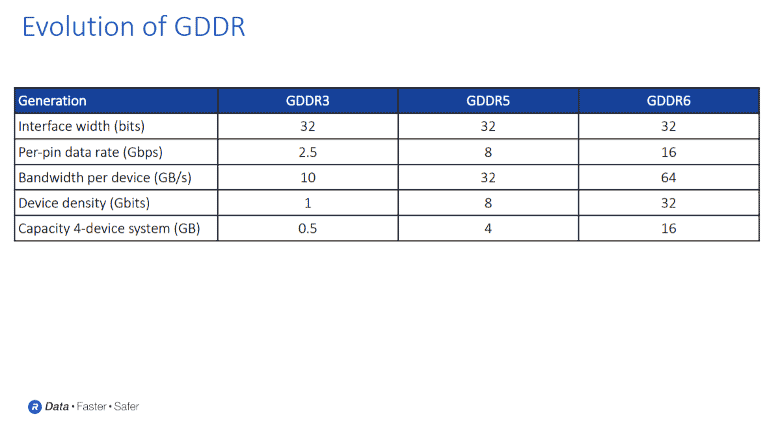
“You handle these with your more traditional PCB type manufacturing process. But 16 gigabits per second is very high speed – and four or five times higher than traditional DDR. So, you do have to be very careful when you design with GDDR6 from a signal integrity standpoint.”
As Ferro notes, there are graphics cards that have anywhere from 10 or 11 GDDR6s on a board to deliver very high bandwidth.
“Most GDDR systems are more bandwidth intensive in density, but you do have some options for additional density,” he elaborates. “With GDDR, the current density goes up to about 32 gigabits per device. GDDR6 also has a mode known as clamshell, which allows you to put two GDDR6s on a board opposite each other to give you double density. GDDR provides lots of flexibility for performance.”
GDDR6 Memory System: Taking A Closer Look
The slide below, says Ferro, offers a close-up look at a GDDR system.
“The GDDR is connected to your processor through a traditional PCB at 16 gigabits per second. However, you do have to be careful about your PCB materials and the physical design and placement of the signals,” he cautions.
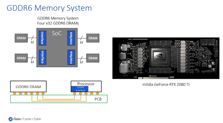
“With GDDR6 running at high speeds, you have to keep an eye on signal integrity. You must take care to avoid a crosstalk and you have to think about issues like insertion loss. You also have to work very closely with your DRAM provider and your physical PHY provider who should provide reference information on how to carefully design those systems.”
Ferro also highlights the NVIDIA GeForce card in the slide above.
“Up in the top right, you have a block diagram of a GDDR system that has four GDDRs. You can see the 32-bit interfaces and this type of system gives you 256 gigabytes of processing. So that is very good for applications like different AI accelerators – where you can implement a PCIe card or even AI in automotive ADAS systems. 256 gigabytes will give you very good performance if you’re implementing an application like a level two or level three ADAS,” he adds.
GDDR6: Benefits and Challenges
As Ferro notes, GDDR6 offers very high bandwidth, good latency, and is well understood from an engineering standpoint. However, he emphasizes that system designs with GDDR6 must take potential signal integrity issues into account.
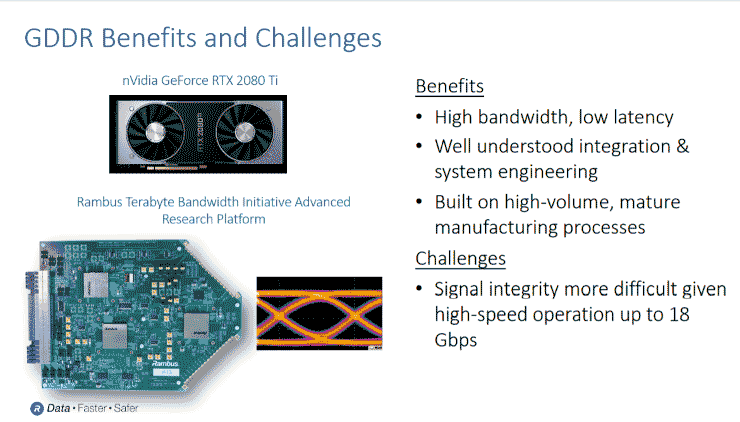
“There are GDDR6 systems even now that are pushing the speed limit beyond 16 gigabits per second. As well, some companies have announced 18 gigabits per second. So, the signal integrity challenges are only going to become more challenging,” he states. “Working closely with the DRAM and the PHY manufacturers are going to be critical for customers designing their PCBs. GDDR6 speeds will continue to push up into and beyond 18 gigabits per second range. The need for bandwidth is not going away, and we’re seeing constant pressure from the industry to move faster and faster with these systems.”
In summary, says Ferro, the demand for higher processing power and more memory bandwidth will only become more pronounced in the coming years.
“Today, the CPU is outstripping the ability of the memory to keep up. So, there is a lot of pressure on the memory suppliers to continue to grow the bandwidth,” he explains. “In particular, we’re looking at a higher bandwidth on the AI training side, which is where HBM is being used. We’re seeing HBM continue to push for higher and higher speeds to keep up with the needs of AI training, while GDDR6 is being used for AI inference.”
As the industry sees more and more processing power pushed out into the network and performed locally, higher GDDR speeds and high-speed memory interfaces will be necessary to support AI inference algorithms and applications such as automotive ADAS.
“This is why we are working very closely with the industry, with customers, with DRAM manufacturers, processors, all the way across the entire industry to look at memory architectures that can service the need of the growing amount of data in the system,” he concludes.

Leave a Reply