GLOBALFOUNDRIES has demonstrated silicon functionality of a 2.5D packaging solution for its high-performance 14nm FinFET FX-14™ integrated design system for application-specific integrated circuits (ASICs).
According to Kevin O’Buckley, VP of ASIC product development at GF, the 2.5D ASIC solution includes a stitched interposer capability to overcome lithography limitations and a two terabits per second (2Tbps) multi-lane HBM2 PHY, developed in partnership with Rambus. Building on the 14nm FinFET demonstration, the solution will be integrated on the company’s next-generation FX-7™ ASIC design system built on GF’s 7nm FinFET process technology.

Image: Semiconductor stock illustration
“With the tremendous advances in interconnect and packaging technology that has occurred in recent years, the line between wafer processing and packaging has blurred,” said O’Buckley. “Incorporating 2.5D packaging into ASIC design boosts performance beyond scaling and is a natural evolution of our capabilities. It enables us to support our customers in a one-stop end-to-end fashion, from product design all the way through manufacturing and testing.”
Luc Seraphin, senior vice president and general manager, Memory and Interfaces Division at Rambus, noted that Rambus’ memory PHY is targeted at high-end networking and data center applications performing the most data-intensive tasks in systems requiring low-latency and high-bandwidth. The PHY is compliant with the JEDEC JESD235 HBM2 standard, supporting data rates up to 2Gbps per data pin, enabling a total bandwidth of 2Tbps.
“We strive to deliver comprehensive HBM PHY technologies that will enable data center and networking solution providers to meet today’s most demanding workloads and take advantage of compelling market opportunities,” Seraphin explained. “Our collaboration with GF combines our HBM2 PHY with their 2.5D packaging and FX-14 ASIC design system and provides a fully-integrated solution for the industry’s fastest-growing applications.”
As we’ve previously discussed on Rambus Press, HBM is a high-performance memory that features reduced power consumption and a small form factor. More specifically, it combines 2.5D packaging with a wider interface at a lower clock speed (as compared to DDR4) to deliver higher overall throughput at a higher bandwidth-per-watt efficiency for high-performance computing applications.
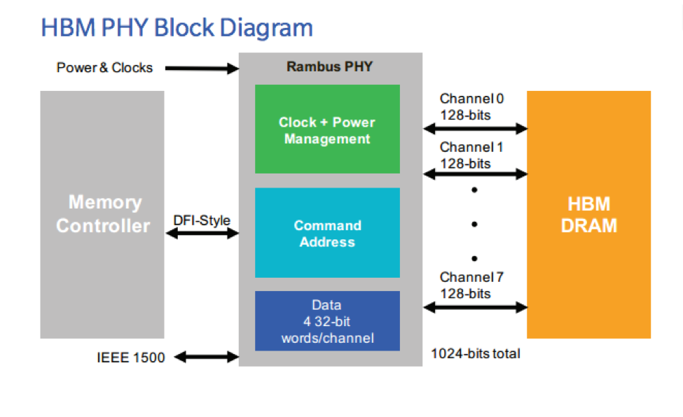
It should be noted that Rambus recently announced the availability of its new High Bandwidth Memory (HBM) Gen2 PHY. Designed for systems that require low latency and high bandwidth memory, our HBM PHY is built on the GLOBALFOUNDRIES advanced 14nm Power Plus (LPP) process technology. The PHY – which is fully compliant with the JEDEC HBM2 standard – supports data rates up to 2000 Mbps per data pin, resulting in a total bandwidth of 256 GB/s. The interface features 8 independent channels, each containing 128 bits for a total data width of 1024 bits, as well as support for a stack height of 2, 4 or 8 DRAMs.

The PHY is designed for a 2.5D system with an interposer for routing signals between the DRAM and PHY. The combination of signal density and stacked form factor requires special design consideration. To enable easy implementation and improved flexibility of design, we perform complete signal and power integrity analysis on the entire 2.5D system to ensure that all signal, power and thermal requirements are met. The HBM Gen2 PHY – delivered as a fully characterized hard macro – includes all necessary components for robust operation, such as IO pads, PLL, clock distribution, transmit and receive paths, control logic, power distribution and electrostatic discharge (ESD) protection circuitry.
Key Rambus HBM Gen2 PHY product highlights include support for DRAM 2, 4 and 8 stack height, a DFI-style interface to the memory controller, 2.5D interposer connections between the PHY and DRAM, a validated memory controller interface, support for wafer-level and interposer testing, as well as availability with LabStation™ Validation Platform for enhanced bring-up and validation.
Additional features include a flexible delivery of the IP core (works with ASIC/ SoC layout requirements), 8 channels and 16 pseudo-channels, selectable low-power operating states, programmable output impedance, pin programmable support for lane repair, ZQ calibration of output impedance, IEEE 1500 test support, SSO noise reduction, micro-bump pitch matched to the DRAM pitch, east-west orientation (PHY can be placed in corner of die) and a register interface for state observation.
Interested in learning more about Rambus’ HBM Gen2 PHY? You can check out our product page here and download our product brief here.
