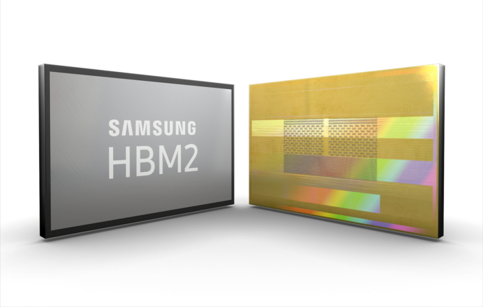
Samsung ramps volume production of 8GB HBM2
Earlier this month, Samsung confirmed an increase in production volume of its 8-gigabyte (GB) High Bandwidth Memory-2 (HBM2) to meet growing market needs across a wide range of applications including artificial intelligence, HPC (high-performance computing), advanced graphics, network systems and enterprise servers.

Image Credit: Samsung
According to Samsung, the 8GB HBM2 consists of eight 8-gigabit (Gb) HBM2 dies and a buffer die at the bottom of the stack, which are all vertically interconnected by TSVs and microbumps. With each die containing over 5,000 TSVs, a single Samsung 8GB HBM2 package has over 40,000 TSVs. The utilization of so many TSVs, including spares, ensures high performance, by enabling data paths to be switched to different TSVs when a delay in data transmission occurs.
HBM in GPUs
As AnandTech’s Anton Shilov reports, Samsung began mass production of 4-Hi HBM2 KGSDs with 4 GB capacity and 2 Gbps data rate per pin in early 2016.
“These chips have been used to build various solutions based on NVIDIA’s GP100 and later GV100 GPUs aimed at HPC and similar applications,” Shilov writes. “The company also started to manufacture HBM2 KGSDs with 8 GB capacity in 2016 and so far, Samsung is the only company to publicly announce that they can mass-produce 8 GB HBM2 KGSDs.”
Why HBM?
According to Semiconductor Engineering’s Ann Steffora Mutschler, HBM2 has continued its steady rise as a viable contender in the memory space. More specifically, HBM is finding its way into leading-edge graphics, networking and high performance computing systems. High-bandwidth memory may also find a role in deep learning, artificial intelligence, convolutional neural networking, fully autonomous vehicles, as well as additional advanced applications that demand massive bandwidth and low power.

“HBM enables lower power consumption per I/O and higher bandwidth memory access with a more condensed form factor, which is enabled by the stacking memory dies directly on top of each other and sharing the same package as an SoC or GPU core using a silicon interposer,” she explains. “Each pin drives a much shorter trace, and runs at a lower frequency, which in turn results in significantly lower switching power.”
High-bandwidth performance gains, says Mutschler, are achieved by a very wide I/O parallel interface.
“HBM1 can deliver 128GB/s, while HBM2 offers 256GB/s maximum bandwidth. Memory capacity is easily scaled by adding more dies to the stack, or adding more stacks to the system-in-package,” she adds.
HBM: Moving memory closer to the processor
As noted above, HBM moves memory closer to the processor using a fatter data pipe, which effectively speeds up data throughput, reduces the amount of power necessary to drive a signal and cuts RC delay. According to Frank Ferro, a senior director of product management at Rambus, high-bandwidth memory was originally seen by the graphics companies as a clear step in the evolutionary direction of memory for GPUs.
![]()
However, the networking and data center community ultimately realized HBM could add a new tier to the memory hierarchy. As a result, high-bandwidth design activities have accelerated across multiple market segments.
This is because HBM bolsters local available memory by placing low-latency DRAM closer to the CPU. Moreover, HBM DRAM increases memory bandwidth by providing a very wide interface to the SoC of 1024 bits. Meaning, the maximum speed for HBM2 is 2Gbits/s for a total bandwidth of 256GB/s. Although the bit rate is similar to DDR3 at 2.1Gbps, the 8, 128-bit channels provide HBM with approximately 15X more bandwidth. In addition, four HBM memory stacks (for example), each with 256GB/sec in close proximity to the CPU, provides both a significant increase in memory density (up to 8Bb per HBM) and bandwidth when compared with existing architectures.
Interested in learning more about high-bandwidth memory? You can check out our article archive on the subject here.
