This is the most comprehensive guide to selecting and implementing a HBM2E memory IP interface solution.
Frank Ferro and Joseph Rodriguez, Senior Directors Product Management at Rambus, hosted a webinar at our Rambus Design Summit discussing HBM2 and HBM2E memory technology.
There’s a lot of decisions that need to be made when you’re developing high speed products for AI, and HBM has become the memory of choice. So, we’re going to go into detail and talk about the selection criteria and implementation details for HBM2E memory.
Let’s dive right in!
Slideshare: The Ultimate Guide to HBM2E Implementation & Selection from Rambus
HBM2E Webinar Transcription:
-
-
-
- Exponential data growth mandates increased bandwidth
- HBM2E vs GDDR6: two important memories for AI
- HBM2E 4G announcement
- Choosing the correct memory: comparison data (table)
- HBM2E solution summary
- Interposer reference design
- Rambus HBM2/2E IP market leadership
- HBM2/2E memory interface solution: controller core
- Why choose Rambus HBM2/2E?
- Next steps?
-
-
Exponential data growth mandates increased bandwidth
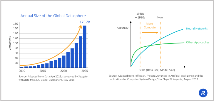 Exponential data growth has really driven everything we’ve done today in the semiconductor industry. The increased need for data is stressing all of our systems. It’s stressing the current computer architectures that we have and it’s really driving innovation to try to do things differently. One of the things that has really become mainstream for computing AI is neural networks and neural networks have been with us for some time now. However, the compute power has not been there to keep up and to really do a good job with neural networks until recently.
Now the computing has caught up. One of the things we’re seeing is that we’ve got plenty of compute power, but the memory bandwidth is now becoming the bottleneck in the system. We’ve got many processors and you just can’t keep these processors fed. The way it’s being done today is using CPU and GPU technology, but as good as the CPUs and GPUs are, to get more efficiency out of your neural networks, custom processors are being developed. Additionally, with those custom processors, you need to have very high memory bandwidth and HBM, as I just said, is really becoming that ideal memory.
Let’s look at some of the specs around HBM.
HBM2E vs GDDR6: two important memories for AI
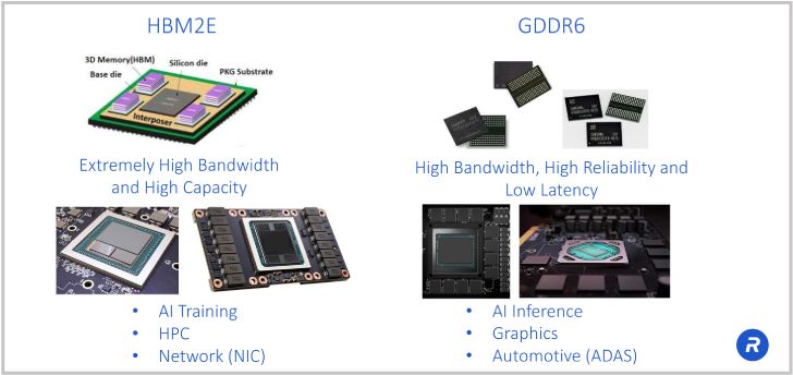 Two of the memory choices you have for AI/ML, are HBM and GDDR6. Both of these technologies were developed for the graphics market.
HBM2, and now HBM2E was developed in order to give you the maximum bandwidth with the current DDR DRAM technology.
So, if you look at the HBM2E picture above, you’ll see stacks of memory.
So, what happening with HBM is you’re taking existing DRAM technology and now you’re configuring them in a 3D stack. The other element is the silicon interposer used to interconnect the processor to the memory stacks.
Each HBM2E device is connected via a 1024-bit wide data interface. With control plane, that rises to over 1700 traces. That’s far more than can be supported on a standard PCB. A silicon interposer makes it possible to print these very fine traces. Use of a silicon interposer is what makes it a 2.5D architecture.
HBM2E utilizes existing DRAM technology combined with 3D and 2.5D manufacturing technologies to deliver extremely high bandwidth.
Another popular memory is GDDR6, again developed for the graphics market, because of its high performance, operating at up to 16 or 18 gigabits per second (Gbps), GDDR6 also looks like a very attractive solution for some AI applications.
You can also see some of those target applications. So, HBM has been a really good solution for AI training applications because that AI training is very data intensive and requires the most bandwidth.
You know, when you’re training these AI algorithms, it could take days and even weeks to get the training right and so you need lots of bandwidth and processing power combined.
Once these models have been trained, then you have another process called AI inference. AI inference takes much less compute power. It needs more cost efficiency because it’s going to be deployed broadly across various end points where these AIs are going to be implemented and that’s where GDDR6 comes into picture.
Keep on reading:
– HBM2 or GDDR6?
– The Autobahn Lanes of HBM2 and GDDR6
HBM2E 4G announcement
Before I get into the product, Rambus just recently announced our latest achievement in HBM.
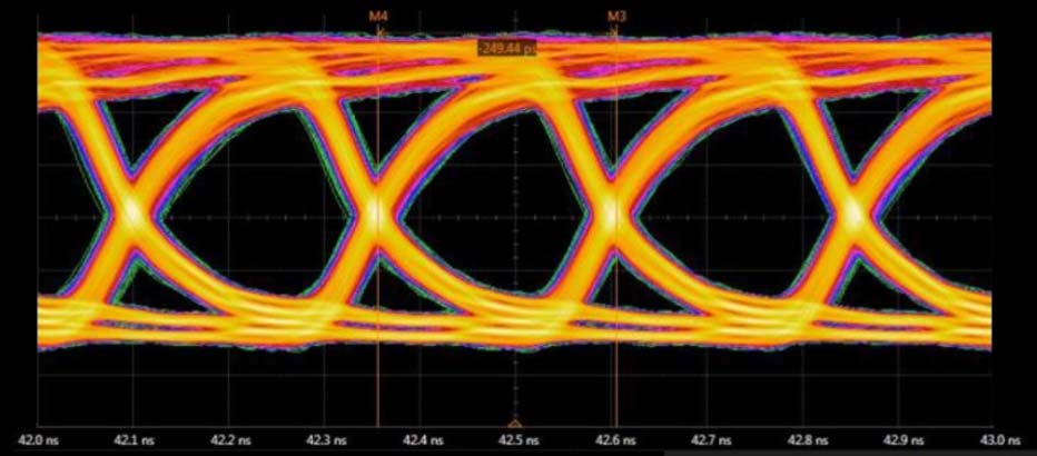
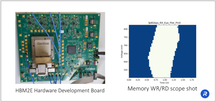
We achieved 4 gigabits per second of performance with HBM2E and this is significant because right now the HBM2E product standard goes to 3.2 Gbps and there have been some DRAM manufacturers that offer performance 3.6 Gbps.
We’ve worked together with DRAM manufacturers, our ASIC partners and manufacturing partners to develop this high-speed test chip. You can see we’ve achieved very clean eyes (see image above). This is the result of doing quite a bit of simulation work to get the interposer design right.
With HBM, you’re passing many thousands of signals through a silicon interposer. Getting that design right in terms of the crosstalk and insertion loss is very critical.
Rambus is renowned as a signal integrity company and our ability to continue to lead the industry with the highest speed memory interfaces is just shown here as we achieve 4 Gbps performance for HBM2E.
As I just mentioned, companies that are developing AI hardware, need more bandwidth. So, the ability to continue to push forward and get the maximum bandwidth out of HBM is very critical.
Choosing the correct memory: comparison data (table)
In this table, we show selection criteria for different memories and I’ve introduced a few different memories on this chart, so you can get a picture of all the memories that can be used for AI.
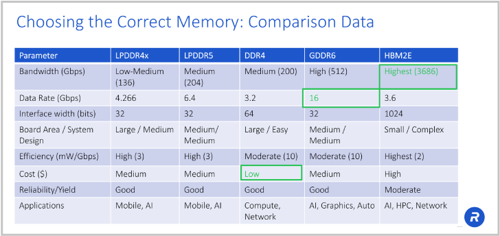
Starting from the left-hand side, we see LPDDR. LPDDR was originally developed for the mobile market with “LP”, standing for low power. With the increasing sophistication of smart phones, the mobile industry too was pressed for greater bandwidth. LPDDR4, for example, was running at 4.2 Gbps. Well, at the time of its introduction, it was one of the fastest memories on the market.
Bandwidth is the product of data rate and interface width. For LPDDR4 that’s 4.266 Gbps data rate times a 32-bit wide interface equals 136.5 Gbps bandwidth. Divide that by 8 to convert bits to bytes, and you get a bandwidth of 17 Gigabytes per second (GB/s). Typically, bandwidth is expressed in GB/s.
Read on:
– AI Requires Tailored DRAM Solutions: Part 1
– High-Performance Memory for AI/ML and HPC: Part 2
LPDDR4, and LPDDR5, work for AI end points and end points, which could be anything from an automotive application, to a home device like an Alexa, where you don’t need a lot of processing power but you do need very low cost and very low power.
However, as we move to the edge of the network, or even up into the cloud, LPDDR can’t deliver enough bandwidth, and you’re going to need solutions like GDDR6 and HBM memory.
DDR is the traditional memory we have in our servers and PCs for main memory. DDR4, runs at 3.2 Gbps, which in a 64-bit wide configuration delivers bandwidth competitive to LPDDR5. But again it falls short of what is needed in emerging AI/ML applications.
Moving to GDDR6, at 16 Gbps data rate, you’re 2.5X the bandwidth of LPDDR5 or DDR4. And we have demonstrated, we can take GDDR6 operation even higher to 18 Gbps.
With HBM2E running at 3.6 Gbps over a 1024-bit wide interface, you can deliver bandwidth of 3.7 terabits per second, that’s more than 18X the bandwidth of LPDDR5 or DDR4! So why wouldn’t you always use HBM2E? Well, the need of an interposer makes for a more complex and higher cost solution. So, you need to look at the trade-offs of price and performance.
Rambus’ Steven Woo Explains GDDR6 – HBM2 Design Tradeoffs (SemiEngineering)
HBM2E checks a lot of boxes. You’ve got the smallest area. You’ve got excellent power efficiency because you’re running at a “relatively slow” speed of 3.6 gigabits per second. You’re going very wide and slow, but you do have more complexity when dealing with 3D and 2.5D structures, so the manufacturing cost is going to be higher.
If you don’t need all the bandwidth of HBM2E and you want to use more traditional manufacturing methods, just die down on PCB. With GDDR6, you leverage traditional high-volume manufacturing processes to deliver the best performance of any of the 2D memory alternatives.
HBM2E solution summary
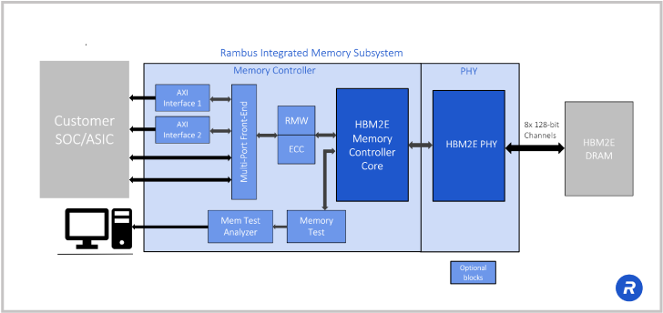
Here you can take a look at the Rambus HBM2E solution. In the center in light blue, you can see our HBM2E memory PHY and controller. This is a complete memory subsystem for HBM2E. The PHY is provided as a hardened, complete, timing-closed macro and we validate that with our HBM2E memory controller.
The combination of PHY and memory controller really simplifies the engineering effort as you’re developing your memory subsystem. Rambus takes care of a lot of the heavy lifting regarding the memory and our memory controller has popular interfaces to the SoC or ASICs in the system. One of the advantages of working with Rambus is that we have a lot of production experience. As I’ll show you in a moment, we have a number of HBM designs that have been in production for a long time.
And again, when you’re purchasing IP, having a production-tested IP is very critical.
We want you to know that it’s going to work right the first time. The other unique thing about Rambus is we don’t just provide IP, we provide complete system design support.
We provide the reference design for the interposer and the package. This again is a huge boost to companies developing AI hardware, because we take you more than three quarters of the way there. When we give you the design, you get a reference design for the interposer, we give you design recommendations on the package, and you get a complete memory subsystem.
Another big, big advantage.
Finally, we provide a tool called Lab Station, a very advanced tool, developed over the last 25 years by Rambus signal integrity experts, that allows full characterization of the memory interface.
Also, it works with your system for bring up. For example, if you’ve got an ASIC that’s powering up for the first time, once you give the PHY and controller a clock signal, then Lab Station will allow you to look at the interface between the DRAM and the physical layer and our PHY, and get that up and running and debugged even while your ASIC is being debugged.
It’s a very powerful solution.
Of course, from the feature side, we support all the standard features of the JEDEC spec for HBM2/2E at speeds all the way up to 4 Gbps and supporting all the different vendors’ HBM2/2E DRAMs. We support features like lane repair. There’s an IEEE 1500 test support that’s part of the standard.
Interposer reference design.
Interposer Reference Design
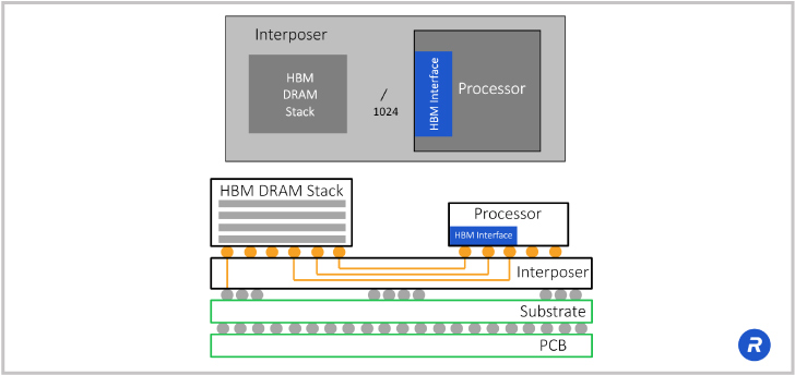
I also mentioned the interposer reference design and as you can see here, I’ve talked a lot about the interface between the processor and the DRAM stack.
So, you can see we have a simplified block diagram where a processor with the HBM interface, and then you can see these orange color signal traces going through the silicon interposer and then these go over to the DRAM stack.
How do you design those signal traces going through the interposer?
There are quite a few HBM design challenges that you have to be aware of when designing an interposer. For example, how long can you make these signal traces? What is the spacing of these traces? What is the thickness of the metal? How many metal layers are there? Where do you place the ground layers?
The answers differ depending on the type of implementation. They are different depending on the process node used. Rambus has reference designs for all the major manufacturers and for the different types of systems that you’re going to be designing. We’ve got extensive production experience, and we’ll work with you on understanding your design. We’ll provide channel simulations, recommendations and feedback on how that interposer design should be implemented.
Rambus HBM2/2E IP market leadership
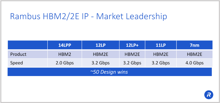 We have a complete and configurable HBM2E memory solution with our controller and associated add-on cores. It’s broadly deployed in over 50 customer designs, as well as several test chips. We’re able to help you with all your design, your architecture, any questions about your system interposer design.
HBM2/2E memory interface solution: controller core
HBM2E offers unrivalled bandwidth thanks to data rates up to 4.0 Gbps. AI/ML also needs high memory capacity, and HBM2E supports 12-high DRAM stacks and can handle 24 gigabit densities per channel.
To make use of the memory capacity and bandwidth, you can configure the Rambus memory controller to the exact memory patterns and traffic sizes of your application. For instance, if you have a very confined, small 32-byte memory accesses at a time, we can configure a dual memory controller solution for that. We can tune the controller to your requirements to meet your power with lower number of gates or higher efficiency or having access to finer grained blocks of memory.
We’ve also added some many great features for RAS, reliability, availability, and serviceability, including ECC, and recently added ECC scrubbing.
We have full featured test support and deliver the controller fully integrated and verified with the PHY.
We can also help you with your testing.
In addition to hardware-based validation, we also have an extensive factory-based verification environment using UVM.
We use the Samsung and SK Hynix memory models, as well as the Avery design systems, memory models and monitors.
You can be assured that you’re not going to spend time debugging the PHY and controller interaction. We deliver to you a high quality, re-usable IP with integrated PHY and controller. Our solution is a mature, full-fledged controller solution with a track record of 100% first-time right delivery performance.
Why choose Rambus HBM2/2E?
In summary, Rambus is the clear choice for your next design requiring HBM2/2E memory.
- We’re the market leader with over 50 customer designs. We’re the performance leader and the only IP supplier to achieve 4 Gbps
- We offer a fully integrated solution of PHY and controller that has been validated in silicon.
- We have 100% first-time silicon success.
- We provide interposer and package reference designs to reduce your design effort and reduce risk.
- We offer the Lab Station development environment to accelerate bring up
And we support you with the industry-leading technical expertise during pre-sales, post-sales and bring-up.
Next steps?
To learn more about HBM2E and all our interface IP solutions, please contact us here and request a meeting with one of our dedicated sales specialists.
Similar topics:
– All about about HBM and GDDR6
– HBM2 gets an upgrade as semiconductor industry eyes HBM3
– eSilicon Tapes Out 7nm Combo PHY (HBM2/HBM2E/Low Latency) Test Chip
Explore more primers:
– Hardware root of trust: All you need to know
– PCI Express 5 vs. 4: What’s New?
– Side-channel attacks: explained
– DDR5 vs DDR4 – All the Design Challenges & Advantages
– Compute express link: All you need to know
– MACsec Explained: From A to Z

Leave a Reply