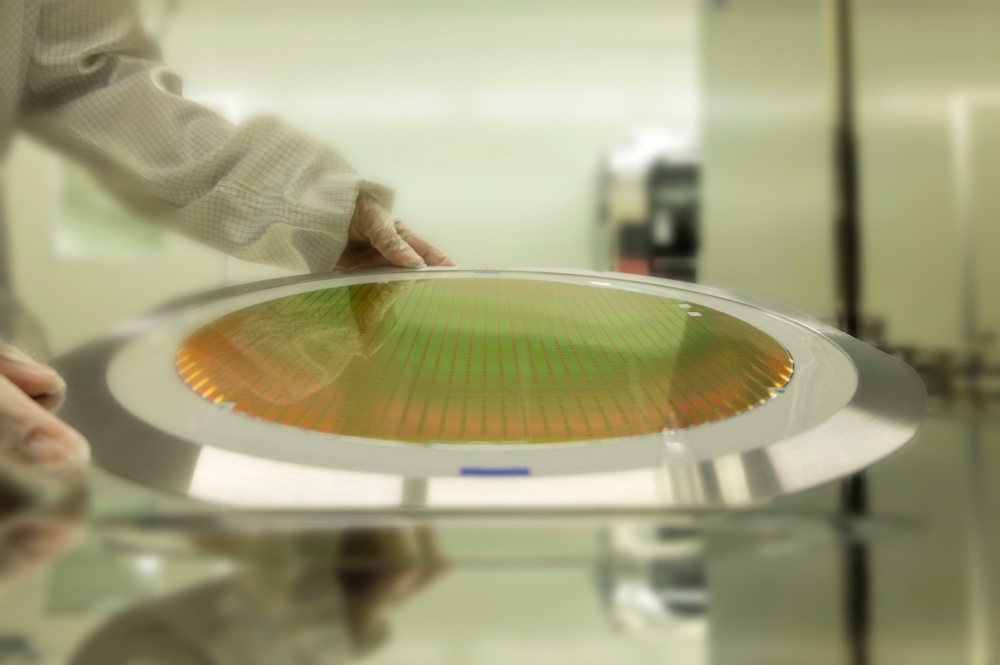
Frank Ferro, a senior director of product management at Rambus, recently penned an article for Semiconductor Engineering about the promises and challenges of 7 nanometers (nm).
According to Ferro, the demand for 7nm is driving expected initial tape-outs from fabs by the end of 2017 – with initial volumes kicking off in 2018 and ramping up by 2019. As expected, silicon fabbed on 7nm nodes will offer a number of benefits for chipmakers, including lower power, higher performance and increased density.

“Implementation at advanced process nodes requires all aspects of the logic design to shrink. This includes a significant decrease in the capacitor size and channel length – which effectively increases logic performance by facilitating faster response times,” he explained. “In addition, dropping to lower nodes enables denser layout and design, as well as more logic and complexity in the same (or reduced) form factor. This is why lower process nodes are particularly important for those architecting next-generation components and blocks such as 56G and 112G SerDes PHYs.”
Nevertheless, as Ferro emphasizes, moving to 7nm presents engineers with a number of signal integrity and manufacturing challenges, including leakage, unstable parasitic structures, defects and imperfections – although the latter two should improve with time as the node matures. Moreover, says Ferro, silicon designed on lower process nodes requires complex multi-physics simulation, emulation and prototyping to ensure successful tape-outs and reliable in-field functionality.
“While chipmakers can extend immersion/multi-patterning from 16nm/14nm to 10nm and 7nm, there is uncertainty about what lies beyond,” he elaborated. “Extreme ultraviolet (EUV) lithography is one method that could potentially help the industry achieve success and high yields at 7nm and more advanced nodes.”
From a PHY IP design perspective, moving towards EUV could reduce the number of masks required at the 7nm node (from multi-patterning practices) and therefore lead to a reduction in engineering design time. As Ferro points out, EUV is currently in development, with at least two major chipmakers slated to implement EUV on 7nm in the 2018 to 2019 timeframe, with high volume use expected by 2020 for even lower nodes.
“In the meantime, here at Rambus we continue to work with our partners and customers to design next-generation silicon across a range of semiconductor device fabrication nodes, including 14nm and 7nm,” he continued. “As an example, GlobalFoundries recently demonstrated silicon functionality of a 2.5D packaging solution for its high-performance 14nm FinFET FX-14 integrated design system for application-specific integrated circuits (ASICs).”
It should be noted that the above-mentioned 2.5D ASIC solution includes a stitched interposer capability to overcome lithography limitations and a 2 terabits per second (Tbps) multi-lane HBM2 PHY, developed in partnership with Rambus. Building on the 14nm FinFET demonstration, the solution will be integrated on GlobalFoundries’ next-generation FX-7 ASIC design system built on 7nm FinFET process technology.
“While there are a number of benefits to shrinking nodes, there are also a number of challenges associated with fabbing silicon at advanced processes such as 7nm and lower,” Ferro added. “Therefore, it is critical for companies to understand when advanced nodes such as 7nm are required and when a more mature semiconductor manufacturing process – such as 28/32nm – would be a more appropriate choice.”
