In part four of this series, we took a closer look at the Roofline model, a modern computer architecture tool that illustrates how applications like artificial intelligence (AI) programs perform on different processor architectures like Google’s tensor processing unit (TPU), NVIDIA’s K80 GPU and Intel’s Haswell CPU. In this blog post, we’ll discuss common memory systems that are used in the highest performance AI applications.

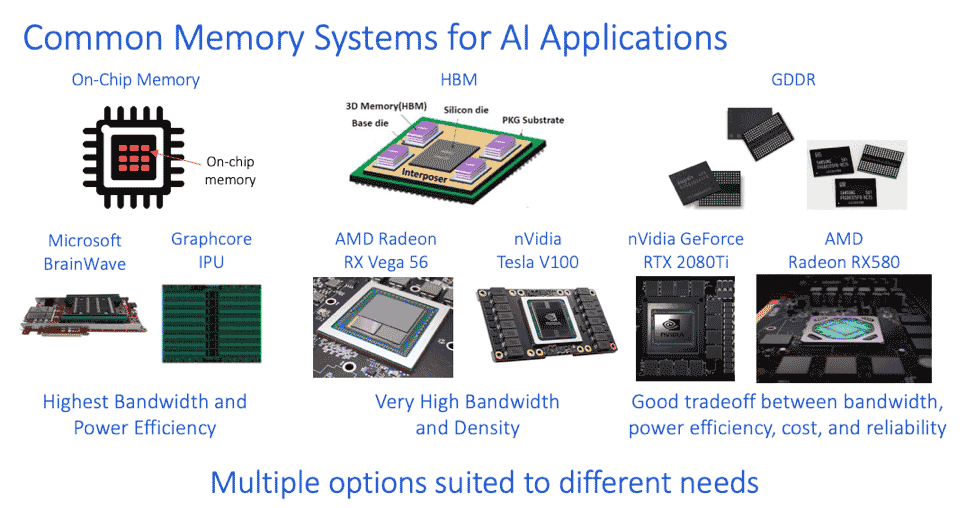
The slide above illustrates the most common types of memory used in high-performance AI applications: on-chip memory, high bandwidth memory (HBM) and Graphics DDR SDRAM (GDDR SDRAM). On-chip memory, in the form of SRAM, is by far the highest bandwidth and most power-efficient solution available today. On-chip memory provides on the order of tens of terabytes a second of memory bandwidth and by far the best power efficiency. However, the tradeoff with on-chip memory is that capacity is low, totaling only a few hundred megabytes per reticle in the best implementations today. If you’re running smaller neural networks, or if you can split your neural network between multiple chips and they can work together, then on-chip memory is a great solution. But if you can’t, external memory must be used.
Currently, the two highest-performing external memories are HBM and GDDR. HBM (shown in the middle of the slide above) is a newer type of memory technology that involves newer stacking techniques both within the memory device, and between components. HBM devices also have many data wires running at a relatively low data rate. Specifically, each HBM stack has 1,024 data wires running at two gigabits per second. That’s more wires than can really be supported on a standard PCB. Therefore, the DRAM device is connected to the SoC using a silicon interposer, where those 1,024 wires can be more finely spaced and etched in the same way that wires are etched into an SoC.
These fine pitch wires etched into a silicon interposer allow us to have a very wide I/O interface running at a very low data rate – and still achieve a very high bandwidth simply through sheer numbers. Put simply, what you can achieve with HBM memory is very high bandwidth at very good power-efficiency. Although not quite as high as the bandwidth provided by on-chip memory, you get much higher memory capacity (8GB today, going higher in the future) in return. So, HBM offers the best bandwidth and power-efficiency for any external memory option that’s available. HBM is used today in solutions from various graphics card manufacturers and some AI chip vendors.
On the right is GDDR memory, which was originally created for the graphics market some 20 years ago. GDDR has undergone several major evolutions, with the latest generation (GDDR6) offering a great trade-off between bandwidth and power efficiency, cost and reliability. GDDR DRAMs rely on the same high-volume manufacturing and assembly techniques used with DDR DRAMs, leveraging this infrastructure and offering a familiarity that reduces cost and implementation difficulty. GDDR DRAMs have 32 data wires (fewer than HBM DRAMs), but run them at much higher data rates, up to 16Gbps in the current GDDR6 standard. The main challenge with GDDR memory systems is the higher data rate, which makes signal integrity and power-efficiency more challenging. Even so, GDDR offers a nice tradeoff between performance, power-efficiency, capacity, cost, and reliability.
Read more of this series:
Memory Systems for AI: Part 1
Memory Systems for AI: Part 2
Memory Systems for AI: Part 3
Memory Systems for AI: Part 4


Leave a Reply