Pre-verified chiplets
Ann Steffora Mutschler of Semiconductor Engineering recently penned an article that explores how the concept of building silicon from pre-verified chiplets is beginning to gain traction – as the semiconductor industry seeks to cut costs and reduce time to market for heterogeneous designs.
“The chiplet concept has been on the drawing board for some time, but it has been viewed more as a possible future direction than a necessary solution,” she explained.
![]()
“That perception is beginning to change as complexity rises, particularly at advanced nodes and as new markets open up that require semi-customized solutions.”
This approach, says Mutschler, could also help re-populate the industry with startups, where mask costs at 10/7nm are well beyond the reach of small companies.
“Startups always have been a driver of innovation, but the number of new companies has dwindled as capitalization requirements rise. And with more chipmakers demanding that IP be silicon-proven, the number of startups has plummeted,” she added.
DARPA’s CHIPS take the lead
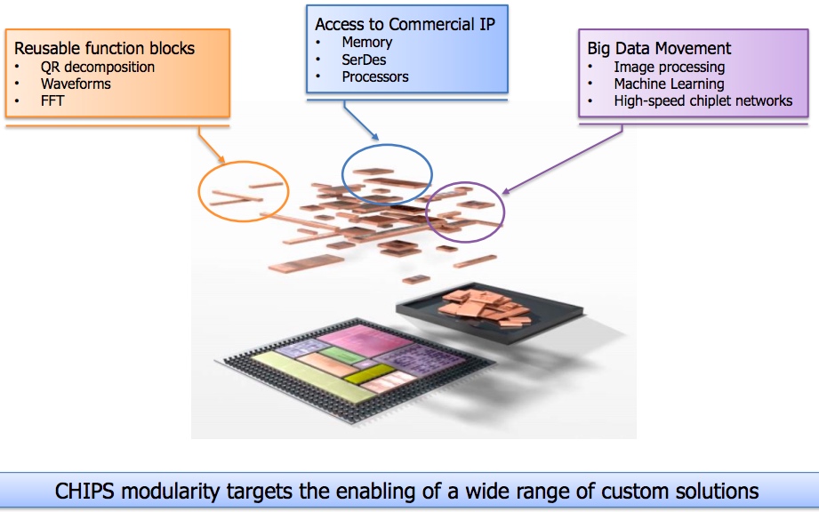
However, this paradigm could change in the near future, particularly as the U.S. Department of Defense’s DARPA branch rolls out its Common Heterogeneous Integration and IP Reuse Strategies (CHIPS) program. CHIPS would see a range of IP blocks, subsystems and chips combined on an interposer in a 2.5D-like package.
As CHIPS Program Manager Dan Green noted in an official 2016 DARPA presentation, CHIPS will develop the design tools and integration standards required to demonstrate modular electronic systems that can leverage the best of DoD and commercial designs and technology.

Image Credit: DARPA
“[CHIPS] really is about enabling the broader community to embrace the ecosystem and we’ve seen a lot of openness to that,” Green told Semiconductor Engineering. “We’ve had conversations with the large players in the space. There is an appetite to understand how to overcome the challenges of design and high NRE for circuit design particularly as you move to the expense of these advanced nodes.”
Towards an era of versatile, plug-and-play chiplets
The CHIPS initiative took center stage this August, when participants from the military, commercial, and academic sectors gathered at DARPA headquarters at the official kickoff meeting for the Agency’s Common Heterogeneous Integration and Intellectual Property (IP) Reuse Strategies program.
As Green detailed during the conference, the program seeks to develop a new technological framework in which different functionalities and blocks of intellectual property — among them data storage, computation, signal processing and managing the form and flow of data — can be segregated into small chiplets, which then can be mixed, matched and combined onto an interposer, somewhat like joining the pieces of a jigsaw puzzle. In fact, says Green, an entire conventional circuit board with a variety of different but full-sized chips could ultimately be shrunk down onto a much smaller interposer hosting a huddle of yet far smaller chiplets.
![]()
“If the CHIPS program is successful, we will gain access to a wider variety of specialized blocks that we will be able to integrate into our systems more easily and with lower costs,” said Green. “This should be a win for both the commercial and defense sectors.”
According to DARPA, specific technologies that could emerge from the CHIPS initiative include compact replacements for entire circuit boards, ultra-wideband radio frequency (RF) systems and fast-learning systems for extracting interesting and actionable data from much larger volumes of mundane data.
SerDes chiplets: The Rambus perspective
Earlier this year, Mohit Gupta, a senior director of product marketing in Rambus’ Memory and Interfaces Division, wrote an article for Semiconductor Engineering titled “From SerDes Chiplets To Die-To-Die Interfaces.” As Gupta explained, after years of steady SoC/ASIC aggregation, a disaggregated approach is now seriously being considered in the form of SerDes chiplets and specialized low-power, application-specific die-to-die interfaces.
“Viable silicon disaggregation can be achieved by moving high-speed interfaces like SerDes to separate die in the form of SerDes chiplets, shifting analog sensor IP to separate analog chips and implementing very low-power and low-latency die-to-die interface through MCM or through an interposer using 2.5D technology,” he elaborated.
![]()
“In addition to leveraging known good die for SerDes in more mature nodes (N-1) or vice versa, disaggregation will facilitate the creation of multiple SKUs, while optimizing cost and reducing risk. More precisely, disaggregation will see SoCs broken out into higher yielding, smaller dies and allow companies to create specific designs with multiple variants.”
Indeed, die-to-die interfaces can more easily accommodate multiple applications across memory, logic and analog technology. In addition, says Gupta, die-to-die interfaces do not require a matching line/baud rate and number of lanes. Moreover, forwarded clock architecture provides low power solution, while FEC may or may not be required depending upon latency requirements.
It should be noted that a number of companies are actively pursuing SoC/ASIC aggregation for switches and other systems. Similarly, the industry is developing ASICs with die-to-die interfaces on leading FinFET nodes, while at least one next-generation server chip is being designed with disaggregated IOs on a separate die.
Interested in learning more about chiplets? The full text of “Chiplets Gaining Steam” by Ann Steffora Mutschler can be read on Semiconductor Engineering here.
