In part one of this three-part blog series, we discussed the low-cost attacks that target security chips such as protocol and software attacks, brute force glitch attacks, as well environmental attacks. In part two, we took a closer look at attacks executed by more sophisticated adversaries. These include side-channel attacks, clocking attacks, fault injection, and infrared emission analysis. In this blog post, we explore the most sophisticated attacks that can target your security chip, such as laser voltage probing, focused ion beam (FIB) editing, reverse engineering, and NVM extraction.
Since these advanced techniques typically originate from national labs or other state funded actors, your adversary will be using advanced failure analysis equipment to gain a detailed picture of the inner workings of your security chip. It is important to understand that bringing a state-of-the-art 10 billion transistor SoC to market in a leading-edge technology node necessitates the use of leading-edge failure analysis equipment to help debug a chip on its path to mass production. Your adversary will have access to this failure analysis equipment and can repurpose it to gain more insight into what a security chip is doing.
In this article:
Laser Voltage Probing
Laser voltage probing is conceptually similar to both the fault injection and infrared analysis we described earlier in this three-part blog series.
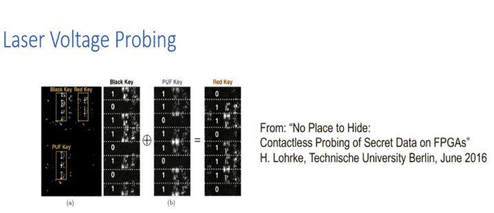
With laser voltage probing, a specific point in a circuit can be measured in a contactless way by zapping that specific node (in the circuit) with an infrared laser. An attacker can subsequently measure the difference in refraction . Even a slight difference in diffraction can alert the adversaries as to whether the data is transitioning from a one to a zero, from zero to a one, or if the voltage is not transitioning it at all. This is an effective technique for reading out the contents of memory buses, the output of physically unclonable functions (PUFs), the output of embedded non-volatile macros, and even some particularly important nodes inside of security core itself.
Laser voltage probing countermeasures are similar to methods we’ve described previously in this three-part blog series. For example, randomness can be used to split the data into multiple components and offset the time at which those components are traversing on a bus. This makes it difficult for the adversary to precisely time their laser voltage probes to extract the data. Randomness – both spatial and temporal (data) – is the most effective countermeasure for laser voltage probe. Since this method involves infrared lasers injected on a node, the previously described techniques of back side metallization can also be a very effective deterrent to this type of attack.
Focused Ion Beam (FIB) Editing
Most companies that have built a chip over the last 30 years probably engaged in some “FIBing.” This is because focused ion beam editing is a very standard debug technique that reaches into the chip to disconnect some signals and reconnect certain logic gates. FIBing is an effective failure analysis tool because it is essentially an additional processing step that can be applied to a chip after fabrication.
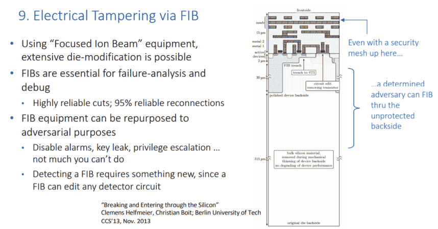
It is almost impossible to prevent a chip from being FIB analyzed. This is because FIB is just another processing step that is applied to the chip after is manufactured. However, this step can be exploited by an adversary to reconnect wires within your chip and deactivate any alarm (generated in the chip). In fact, additional pads can be dropped down onto the chip – and the chip can be repackaged by an adversary to grant access to internal nodes that otherwise would not have been exposed externally before.
The unfortunate reality is that countermeasures for FIB attacks are very difficult to effectively implement. Our Rambus security team is currently researching the use of tamper evidence physical unclonable functions, or PUFs. This will enable the metallization of the chip itself to be fingerprinted when the chip is manufactured. The fingerprint remains a wholly internal portion of a secret key. If an adversary were to FIB into the chip and modify this metallization, the secret key value would be inevitably corrupted, rendering the attacks unsuccessful.
Reverse Engineering
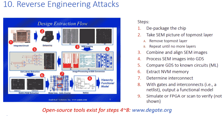
Reverse engineering enables an adversary to destructively decompose a chip, layer by layer, taking very precise scanning electron micrographs that enables an attacker to reconstruct the actual logical netlist. Oftentimes this is done to recover proprietary functions that might be realized within the chip, or to recover read-only memory that has been compiled into a standard cell library circuit within the chip.
Countermeasures for reverse engineering attacks are fairly well known. The basic concept is to corrupt the automatic reverse engineering process by building lookalike or camouflage gates into the netlist. This way, when an adversary takes very careful pictures of what they believe to be a NAND gate, for example, they will discover that it is not actually a functioning NAND gate (because camouflage technology was used to modify the logical operation of that gate). Although it might look identical to a standard cell gate, it performs a different logical operation. So, when your adversary has finished extracting your 100,000 or one million gate circuit, the netlist they will have is incorrect. Because of the camouflage logic, they have no idea which one of the gates is incorrect. This can greatly delay your adversary’s attempt to recovery a proprietary netlist that is hidden on-chip.
Another way of protecting against a reverse engineering attack is a concept known as logic locking. This is similar conceptually to FPGAs which load a bit stream into the circuit – although the circuit does not perform a correct operation until the correct bit stream is loaded. Logic locking is similar, with a large digital signal (perhaps a 256-bit wide signal), loaded to a proprietary function that will not operate correctly until the right signal is applied. This means that if an adversary manages to recover your netlist from the chip, they still need to recover the very small 256-bit file that controls the correct operation of the chip. This method can help mitigate against the more straightforward approaches of reverse engineering attacks.
NVM Extraction
NVM extraction targets the contents of non-volatile memory. Most of the time, secrets inside of a security chip are hidden in a combination of proprietary netlist and NVM contents. An adversary must therefore recover both to make sense of your secret data. Unfortunately, every embedded non-volatile macro has an attack surface on it, and your adversary will be familiar with that type of macro and what type of attacks can be used against it.
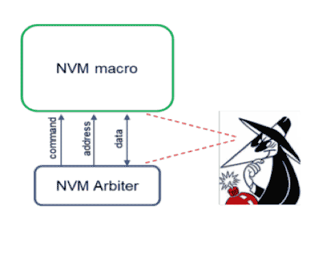
For example, if your NVM macro only has a very narrow data bus, a type of power analysis known as template attacks can be used to recover the data. In addition, if your NVM macro allows secret data to be read and written during a manufacturing state, then your adversary will go after the manufacturing state and try to trick a chip that has already been provisioned with secret data into thinking that it is in the manufacturing state where the data can be read out.
There are even more sophisticated attacks that use scanning electron microscopes to sense the contents of any type of charged based memory, such as EEPROM or embedded flash. Finally, more advanced techniques use the laser voltage probing or FIB attacks we described earlier to monitor the actual data bus of the chip – and perhaps to even take control of the command address portions of the chip to walk the data out of the chip after it has been repackaged.
Countermeasures for this type of attack include a lot of brute force approaches, such as very wide data buses that are much more difficult to repackage and analyze, as well as the previously described countermeasures for both laser voltage probing and FIB attacks.
Rambus Anti-Tamper Technology
Thus far, we have described a number of anti-tamper countermeasures in our three-part blog series. It should be noted that all of our fixed function cores such as AES, SHA and the Public-Key Accelerators include all of the algorithmic countermeasures for wherever algorithm countermeasures are effective, such as in power supply analysis and fault injection countermeasures.
Moreover, our root of trust cores, which are more sophisticated processor-based systems coupled with fixed function cores, include more countermeasures because there are dispatches that can be controlled by the processing elements to, for example, activate ‘first to fail’ logic cores. This ensures these cores are active during execution of the fixed function cores – and makes sure they can randomly stage secure cryptographic events to the cores to thwart timing attacks.
Our anti-counterfeiting line of products include the most countermeasures because these products exist in a chip level form. For these products, we can include some of the more advanced protections against glitch, environmental attacks, and even some more advanced attacks like laser voltage probing and FIB editing of the security chip.
The slide below presents a visual summary of the countermeasures that we have in our security products.
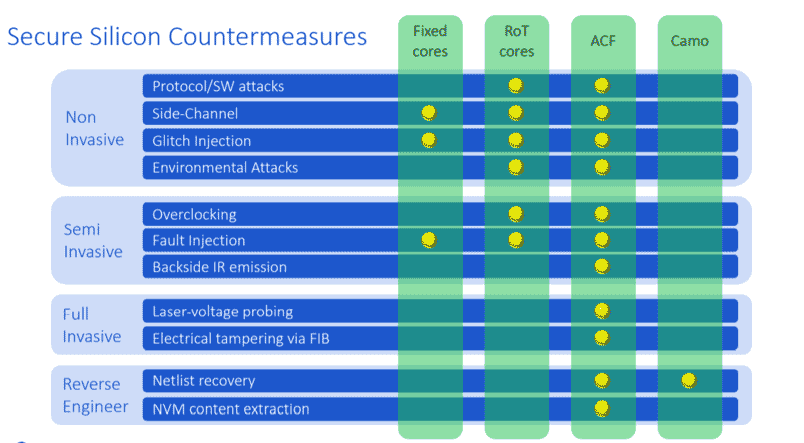
As you can see, the fixed function cores include algorithmic countermeasures for wherever they are appropriate, such as inside channel glitch injection and fault injection protection. Our root-of-trust cores have a wider selection of countermeasures that can be included because of the more sophisticated execution environment. In addition, our anti-counterfeiting solution, (represent by the ACF column), summarizes an inclusion of countermeasures for these attacks. Lastly, our standalone camouflage technology is used to protect against netlist recovery and reverse engineering attacks.
Read more in this series:
Understanding Anti-Tamper Technology: Part 1
Understanding Anti-Tamper Technology: Part 2


Leave a Reply