PCIe 7.0 Retimer Controller with CXL Support
Home > Interface IP > PCI Express Controller IP > PCIe 7.0 Retimer Controller with CXL Support
PCI Express® (PCIe®) 7.0 links operating at 128 GT/s using PAM4 signaling have a reach of up to 13 inches at nominal conditions on standard PCBs. Extending trace routing beyond this distance results in higher first bit error rates (FBER) and reduced link efficiency due to increased link recovery and retransmissions.
As new distributed architectures are deployed in data centers, greater flexibility is desired for chip placement including the need for longer trace lengths. Protocol-aware retimer chips can fully regenerate signals allowing board designers to extend reach and flexibly build various system topologies. The Rambus PCIe 7.0 Retimer Controller provides a complete digital data path solution that delivers best-in-class latency, power and area, and accelerates the time-to-market for PCIe 7.0 retimer chips.
How the PCIe 7.0 Retimer Controller Works
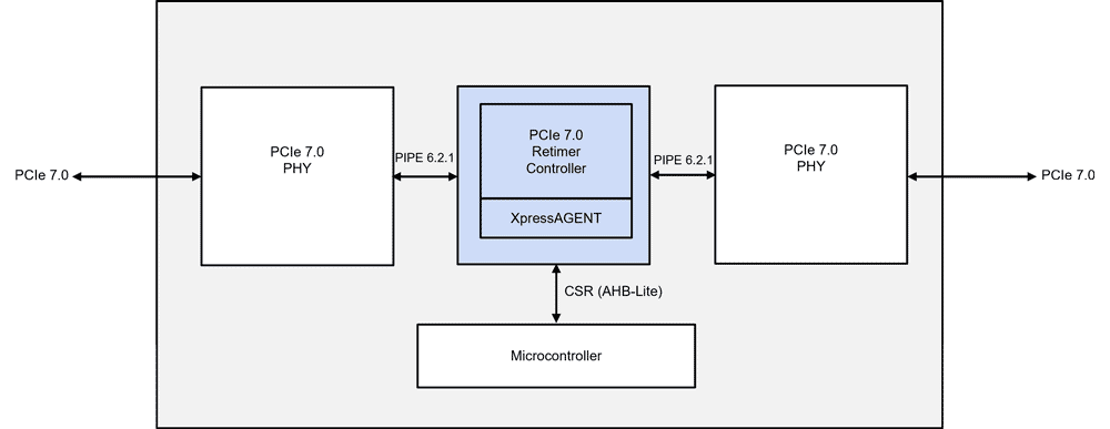
The PCIe 7.0 Retimer provides a highly optimized low-latency data path for signal regeneration. It supports retimer chip PHYs via PIPE 6.2.1 interfaces. The control plane interface is provided via CSR (AHB-lite). The PCIe 7.0 Retimer Controller is CXL protocol aware and supports links using 128 GT/s and lower data rates of PCIe.
Data Center Evolution: The Leap to 64 GT/s Signaling with PCI Express 6.1

The PCI Express® (PCIe®) interface is the critical backbone that moves data at high bandwidth and low latency between various compute nodes such as CPUs, GPUs, FPGAs, and workload-specific accelerators. With the rapid rise in bandwidth demands of advanced workloads such as AI/ML training, PCIe 6.1 jumps signaling to 64 GT/s with some of the biggest changes yet in the standard.
Solution Offerings
- Supports PCIe 7.0 128 GT/s speeds at up to x16 lanes
- CXL 3.0 aware
- Supports PIPE 6.2.1 compatible PHYs
- Optimized for low latency
- Highly-configurable equalization algorithms and adaptive behaviors
- Pre-integrated XpressAGENTTM debug monitor
- Supports up to 4 retimers in series per the retimer protocol specification
IP Files
- IPXACT files for registers
- Software API in C and Python for XpressAGENT (debug monitor)
Documentation
- Retimer IP User Guide
- Getting Started Guide
Reference Designs
- Synthesizable Verilog RTL source code
- Simulation environment and test scripts
- Synthesis project and DC constraint files (ASIC)
Lint and CDC scripts
Advanced Design Integration Services:
- Integration of commercial and proprietary PCIe PHY IP
- Development and validation of custom PCIe PCS layer
- Customization of the Controller IP to add customer-specific features
- Generation of custom reference designs
- Generation of custom verification environments
- Design/architecture review and consulting


